Connection Relationship Between SWD and Chip ISP

2025/09/15 19:55:13 6

SWD (Serial Wire Debug) is a serial interface–based debugging and programming protocol widely used in ARM Cortex microcontrollers (MCUs) and some embedded chips. It is closely related to a chip’s ISP (In-System Programming) functionality and serves as a critical means for online programming, debugging, and firmware upgrading. This article provides a comprehensive explanation of the connection relationship between SWD and chip ISP, including working principles, interface design, application scenarios, and key considerations.

1. Conceptual Relationship between SWD and ISP

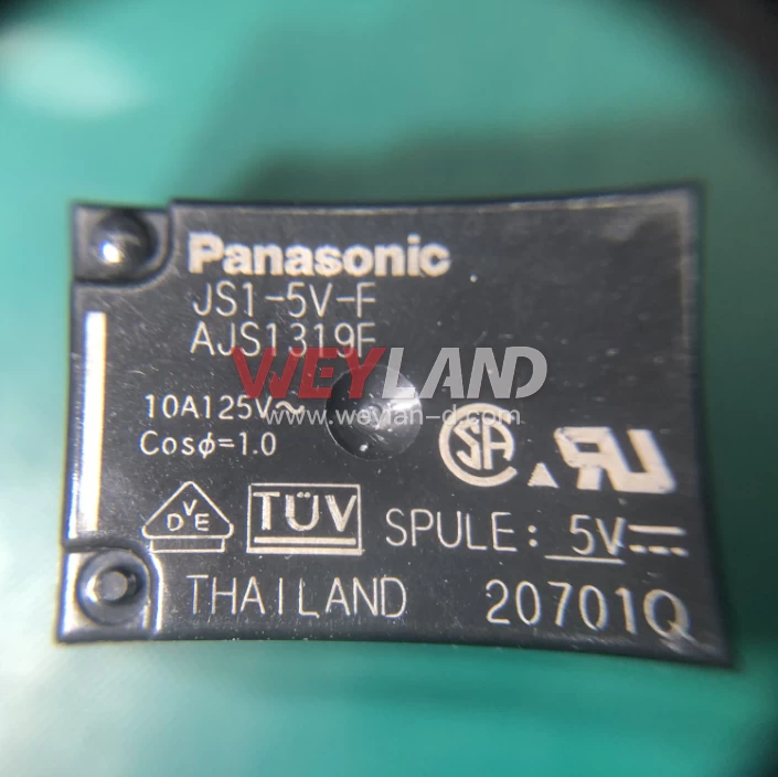
ISP is a feature provided by a chip that allows direct writing, reading, or updating of firmware, registers, and configuration parameters within a system, without removing the chip from the circuit board. ISP supports multiple interface types, such as SPI, UART, JTAG, and SWD, for online programming, firmware upgrades, and parameter tuning.

SWD is a simplified serial debugging interface proposed by ARM, designed to replace the traditional 4–5 wire JTAG interface. SWD uses only two signal lines to perform debugging and programming functions:

  • SWDIO (Serial Wire Debug Input/Output): A bidirectional data line for transmitting debug commands and data.
  • SWCLK (Serial Wire Clock): A clock signal for synchronizing data transmission.

Through the SWD interface, a chip’s ISP functionality can perform online read/write operations on Flash, EEPROM, or on-chip configuration registers, supporting program burning, debugging, and system parameter modification.

2. Connection Principles between SWD and Chip ISP

After power-up or reset, a chip typically enters ISP or programming mode through specific pins. The SWD interface serves as the physical channel for programming and debugging, connecting to the chip’s internal Debug Access Port (DAP). The DAP then accesses on-chip memory and registers via internal buses. The connection relationship can be summarized as follows:

  • Physical connection: SWDIO and SWCLK are connected to the corresponding ports of a programmer or debugger, and the GND pin must be common. Some devices may also require a RESET pin to trigger ISP mode.
  • Logical access: The programmer sends instructions to the DAP via the SWD protocol. The DAP parses the commands and executes read/write operations on Flash or registers, enabling ISP functionality.
  • Voltage levels and timing: SWD lines are usually compatible with 3.3V or 5V logic, with timing controlled by the programmer to ensure reliable data transmission.

Through this connection, SWD acts as the physical interface and data channel for ISP, enabling programming and debugging directly on the system.

3. ISP Functions Achieved via SWD

  • Firmware download and update: ISP can write compiled firmware (HEX or BIN files) to the chip’s Flash via SWD.
  • Register access: Online read/write of on-chip registers for debugging, parameter optimization, and functional configuration.
  • Debugging: SWD allows halting the chip, single-stepping, and monitoring memory or variables to verify program logic.
  • Bootloader operations: SWD can trigger the chip’s bootloader mode for secure firmware upgrades or restoring factory programs.

4. SWD Interface Design and Considerations

  • Wiring: Keep SWDIO and SWCLK lines short to minimize interference; ensure GND is well-connected for signal integrity.
  • Voltage matching: Ensure the programmer’s output levels match the chip’s logic levels to avoid damage.
  • Reset control: Some chips require RESET in combination with SWD to enter ISP mode; timing must follow the chip manual.
  • Debug isolation: In large systems, jumpers or switches may isolate SWD to avoid interference with normal operation.
  • Power management: Chips may enter high-power modes during ISP download or debugging, so a stable power supply is essential.

5. Application Scenarios

  • Embedded development: Online debugging and firmware download via SWD accelerates development cycles.
  • Mass production: SWD enables batch firmware programming to improve production efficiency.
  • Field maintenance and upgrades: IoT devices, smart terminals, or industrial equipment can update firmware and optimize parameters via SWD.
  • Security and testing: SWD combined with ISP allows read/write verification to ensure the correctness of factory firmware.

6. Conclusion

The SWD interface is a key physical channel for implementing a chip’s ISP functionality. Through SWDIO and SWCLK, a programmer can access the chip’s internal DAP to perform online Flash, EEPROM, and register read/write, debugging, and firmware updates. The tight integration of ISP and SWD enhances development efficiency, facilitates field maintenance, supports remote upgrades, and enables mass programming. Understanding the connection relationship, working principles, interface design, and best practices of SWD and ISP is an essential skill for embedded system development, product debugging, and system maintenance.

Statement: This article is reproduced for the purpose of passing on more information.
Please contact us if the source is mislabeled or violates your legal rights.
We will promptly correct and delete, thank you.
Share this post
Recommend Brand:
Subscribe Weyland
Hot Model View More
Microchip
32KB 2.5KB FLASH 26 ...
Microchip
128Kbit I2C SOP-8 E...
ST
4KB 2.7V~5.5V 256Byt...
Microchip
±30% SPI 2.7V~5.5V 1...
Infineon
100V 57A 200W 25mΩ@1...
Microchip
14KB 1.8V~5.5V PIC 3...
Littelfuse
16V 1.5A 100A 2.8A 1...
Panasonic
220uF 6.3V 25mΩ@100k...
YAGEO
250mW Thick Film Res...
Panasonic
AgSnO2 5V 10A SPDT (...
ISO 9001: 2008
ISO 13485
ISO 14001
ISO 28000: 2007
ISO 45001:2018
ESD
Contact Us
  • [email protected]
  • 7500A BEACH ROAD #04-307 THE PLAZA SINGAPORE (199591)
  • RM 705.7/F.FA YUEN COMM BLDGNO.75-77.FA YUEN STREET.MONGKOK.KLN.HONG KONG
Payment Method
Subscribe
Subscribe
Copyright © 2023-2025 www.weylan-d.com