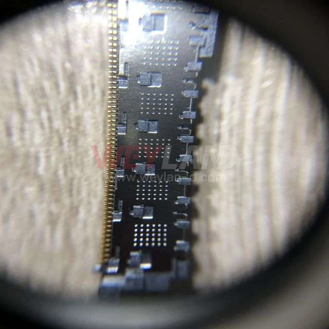
MAXSCEND has obtained a number of patents in RF technology reserve. For example, it has obtained the utility model patent authorization “Chip Packaging Structure and RF Module Device”, which establishes electromagnetic shielding wall between different chips to play the role of electromagnetic shielding, avoiding the occurrence of electromagnetic wave mutual interference between different chips inside the plastisol body, and avoiding the entry of plastisol material and other objects into the cavity by covering the protective film to protect the filter chip By covering the protective film, objects such as plastic sealing material can be prevented from entering the cavity to protect the fork-finger transducer below the filter chip, and the structure and manufacturing process are simple and the cost is relatively low.
As of September 5, 2024, MAXSCEND has obtained a number of patents. The following are some of the patents related to RF technology:
- “A kind of RF module and RF device": Authorization Notice No. cn220829959u, application date is August 2023. The utility model can realize the electromagnetic shielding function and also reduce the difficulty of controlling the height of the half-cut process.
- “A kind of RF front-end port multiplexing circuit": authorized bulletin number cn109302203b, the application date is November 2018. It multiplexes a port of an RF front-end device into an RF port and a control port, realizing two applications for the same port and effectively solving the problem of insufficient number of ports.
- “An RF switch chip": authorization announcement number cn108807343b, application date July 2018 The problem of large size of the existing RF switch chip is solved, and the design is compact and small, thus improving portability performance, wider adaptation range, and lower cost.
- “Radio frequency switch and its control method": Publication No. cn117674784a, filed in August 2022. It can solve the problem that RF switches cannot combine fast switching speed with high quality factor.
- “RF module packaging structure and method for making the same": Publication No. cn117637497a, filed in November, 2023 It is capable of reducing electromagnetic coupling and interference inside the system-level packaging module, as well as shielding electromagnetic interference outside the system-level packaging module, improving the quality and reliability of signal transmission, and also improving process stability, processing operation efficiency, while taking into account low cost, and is suitable for mass production and application.
- “A low-noise amplifier with adjustable current and gain": Authorized Publication No. cn116505895b, filed March 2023 Flexible gain adjustment and current adjustment can be realized to meet the matching and noise requirements at different gains, thus enabling the receiver system to have a large dynamic input range, as well as better current utilization and linearity in different gain modes.
- “Chip Packaging Structure and RF Module Device": Patent Application No. cn202322472352.4, Date of Authorization May 14, 2024 The establishment of electromagnetic shielding wall between different chips plays the role of electromagnetic shielding to avoid mutual interference of electromagnetic waves between different chips inside the plastic package; by covering the protective film, it avoids plastic material and other objects from entering the cavity and protects the fork finger transducer below the filter chip, and the structure and manufacturing process are simple and low cost.
The company has formed a number of invention patents and utility model patents in the field of RF switches, RF low-noise amplifiers, RF filters, WiFi Bluetooth products and so on. These patents are a strong guarantee for the competitive advantages of the company's products, and also lay a technical foundation for the company to maintain product innovation.

 Search
History
Search
History  Hot
recommend
Hot
recommend


 New Posts

.9246509.png)


 [email protected]
 7500A BEACH ROAD #04-307 THE PLAZA SINGAPORE (199591)
